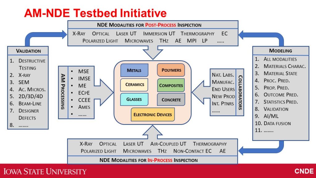
The importance and impact of Additive Manufacturing (AM), spanning almost all national and global industrial manufacturing processes cannot be overestimated. The ability to rapidly and reliably manufacture parts and components has transformed the way we currently look at manufacturing enterprise. Additive manufacturing however desirable, brings with itself significant inspection challenges of manufactured parts that take a plethora of shapes, geometries, sizes and properties (e.g., metals, ceramics, polymer-matrix composites, etc.).
In this respect, the following excerpts from a recent report entitled – Rapid Reliability Assessment of Safety-Critical and Emerging Technologies: Next Generation Nondestructive Evaluation1, succinctly describes the challenges facing AM and four identified key areas in which focused research is needed to overcome these challenges.
“In-Process Additive Manufacturing – Quality and performance evaluation during AM processes is critical for both anomaly detection and prevention. A key barrier to the broad realization of AM, especially for safety-critical parts, is a poor understanding of the anomalies present in an additively manufactured part and their effect on lifetime part performance. This understanding must evolve within the context of the part’s functional requirements, so that manufacturers can determine when an anomaly becomes an unallowable defect. Detecting defects in-situ during the AM process could provide a host of benefits, including:
- Early detection of unallowable defects so that building parts can be canceled early, reducing waste;
- Real-time feedback and control of the AM process to produce higher quality parts with fewer anomalies;
- In-situ repair of defects during manufacturing;
- Better correlation of in-process data with final part condition;
- Better understanding of the microstructure of the part, especially of internal portions that are difficult to assess; and
- Enabling the creation of certifiable parts by AM processes.
AM uses many processes, materials, and raw material forms, which leads to a variety of NDE challenges that are specific to the material and/or process. With polymers, for example, the assessment of shrinkage is complicated. Post-processing, such as hot isostatic pressing, can create defects that must be better understood. Composites, including both polymer-matrix composites and ceramic-matrix composites, are a nascent AM area that is going to be particularly challenging to inspect. Manufacturers have expressed a very strong interest in advancing NDE for metal AM. Better NDE is needed throughout the process—from feedstock evaluation to assessment of powder beds to melt pool monitoring—and for the finished part.
Research into these critical areas is already under way, including with ASTM, which is working with the fabricators industry to develop E07.10 WK62181,e “New Guide for Standard Guide for In-Situ Monitoring of Metal Additively Manufactured Aerospace Parts.” Federal agencies including the United States Air Force, National Institute for Standards and Technology (NIST), Federal Aviation Administration (FAA), and National Aeronautics and Space Administration (NASA),8 as well as the International Organization for Standardization(ISO), ASTM International, American National Standards Institute, and the America Makes Manufacturing USA Center, have held workshops and formed working groups to address the challenges of NDE for AM and have helped to inform critical research directions. The NDE and manufacturing community identified four key areas requiring a research focus:
- Advancement of AM anomaly characterization, including characterization of geometric and microstructural anomalies, relation of anomalies to material and part performance, and definition of allowable ranges for anomaly detectability and acceptability.
- Integration of NDE with feedback, control, and calibration, including real-time in-situ NDE inspection and analysis, control methods that leverage NDE data, AM machine calibration, and correlation of in-process data with final part condition.
- Tools for assessing ceramic-and polymer-matrix composites during AM, addressing the challenges of NDE for multi-material and non-conductive materials.
- Development of NDE technologies for metal powder bed AM that enable assessment and characterization of porous material and high-temperature melt pools.”
Center for Nondestructive Evaluation (CNDE), in cooperation with faculty from various academic departments at Iowa State University (ISU) and scientists at Ames National Laboratory (US Department of Energy) are working together, under an initiative to form a Thrust within CNDE to address a multitude of challenges pertinent to AM processes and in-situ and post-manufacture NDE of parts. This collaboration brings together scientists and engineers contributing to this Thrust through incorporating their unique and diverse NDE modalities (singularly or as a team) and know-how to address these challenges. Some of the specific AM NDE Capabilities and Processing Infrastructure are provided here.
Nondestructive Evaluation (NDE)
PoC: Mr. Z. Zhang
Ultrasonic inspection is a technique that is often utilized in the raw material, intermediate, or in-service inspection of high-performance components in the oil and gas, aerospace, and automotive industries. Metal AM has been investigated by several researchers at CNDE due to industry desire to reliably produce and deploy components made with these processes. The program developed thought leadership in NDE for AM and identified needs that must be addressed including design for inspectability and potential value added by NDE methods at all stages of AM. Ultrasonic testing with a 6 degree of freedom immersion tank examined the effect of surface roughness on the transmitted signals across potentially rough boundaries encountered in AM. This roughness is known to affect detectability of embedded defects, and analytical formulations on the effects of this roughness were verified. Probes and associated hardware can achieve frequencies of up to 25 or 50 MHz with several immersion testing systems.
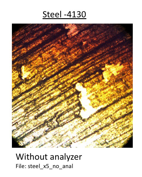
Metal AM is in general analogous to welding or sintering, and as a result, cracking is often a concern. Novel acoustic emissions (passive technique) monitoring methods were developed. This included the associated mounting hardware, multi-sensor signal processing, and diagnosis methods to identify both discrete crack initiation and noise monitoring for broad process monitoring and control in powder bed systems. CNDE also has a storied history of grain morphology characterization, including assessing grain elongation, grain size, and texture development which are known issues in wire-fed systems, particularly. Analytical methods for inversion of ultrasonic data to produce estimates of elongation and grain size are available and ready to be applied. CNDE also has extensive experience with non-contact, air-coupled ultrasonic methods that have applicability to high performance polymeric formulations used in large area AM fabrication methods.
PoC: Mr. D. Barnard
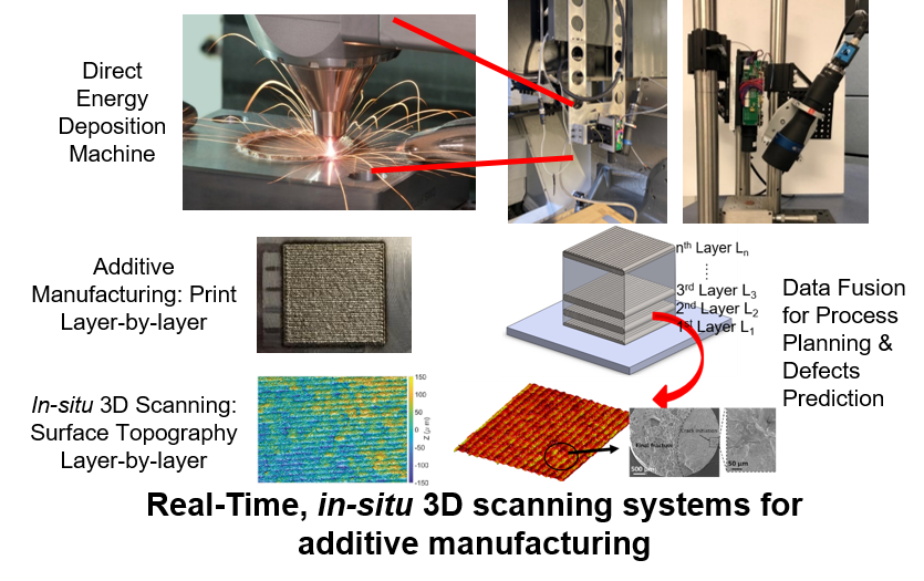
Different from conventional optical techniques that primarily performs post-process/ex-situ surface metrology, this approach focuses on real-time/in-process/in-situ 3D surface metrology. A unique 3D optical measurement system based on the structured light technique using a telecentric lens (US patent #: 10412365) has been developed for this purpose. The uniqueness of this technology is that the 3D topography of the entire printed surface layer can be reconstructed all at once with an accuracy in the few micrometer range, making it feasible to acquire high-fidelity 3D surface data in real-time. An ongoing effort involves developing process monitoring for a Direct Energy Deposition (DED) machine using layer-by-layer 3D surface topography scanning. The goal is to understand the relationship between the layer-wise 3D topography data and some specific defects in additive printing. In addition, having surface topography data of the current printed layer in real-time is extremely beneficial to aid the process planning or corrective actions for the next printing layer.
PoC: Dr. B. Li
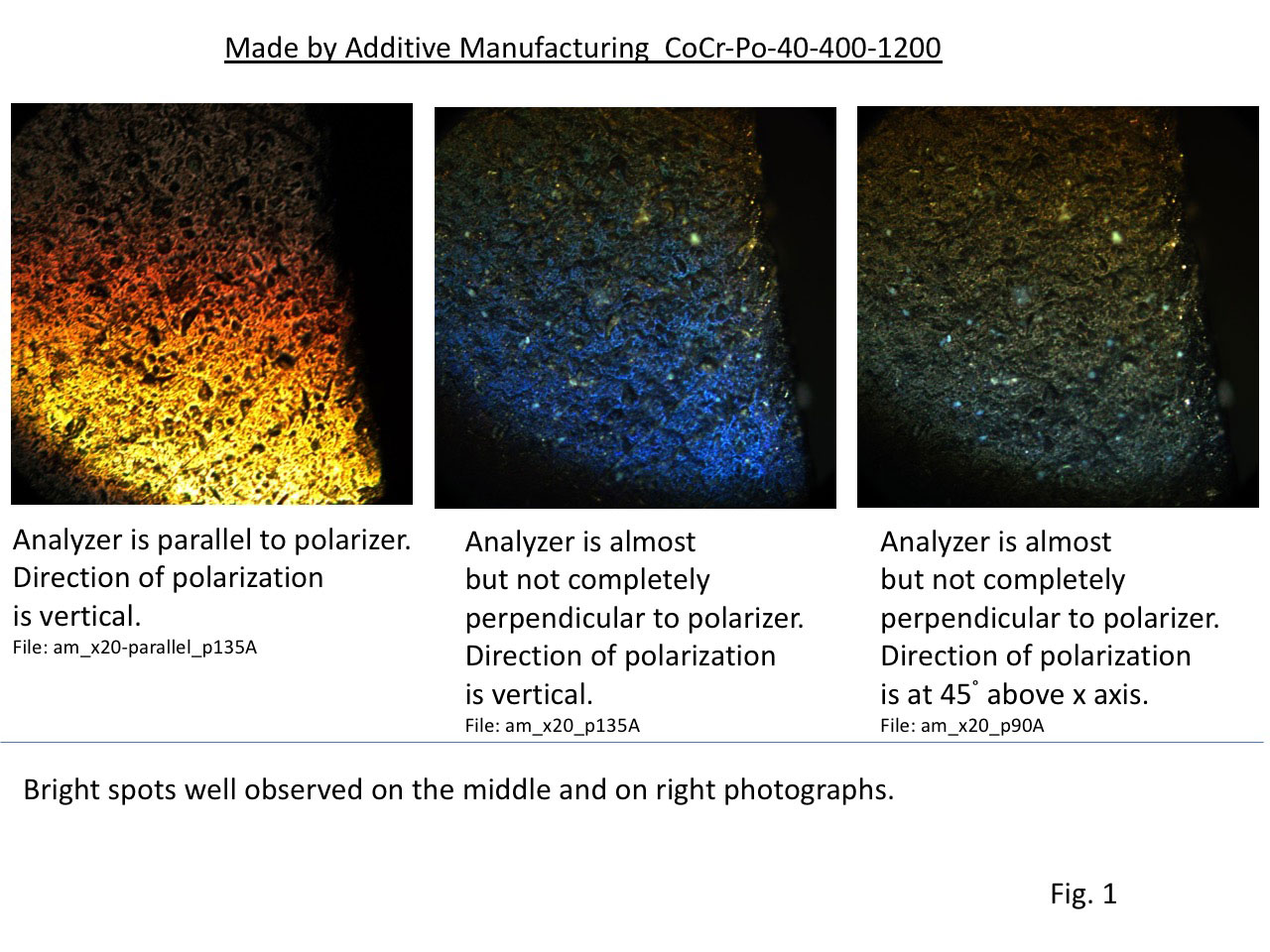
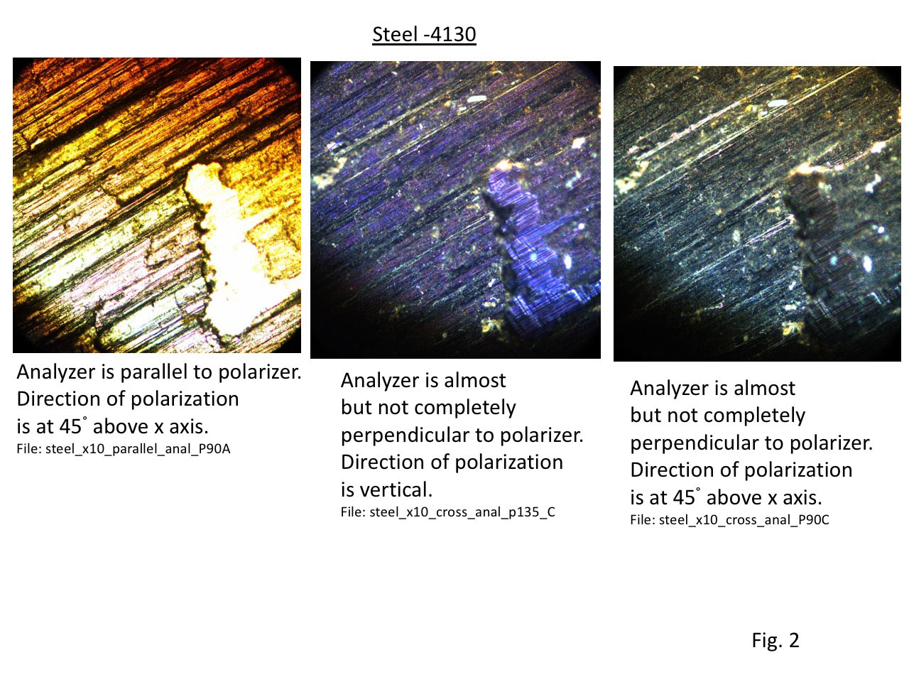
Real-time nondestructive monitoring during the AM process provides opportunity to introduce corrections to the procedure and to obtain information from internal components of AM part without destruction. However, the environment (i.e., high temperature, active chemicals, etc.) in which AM process takes place usually presents certain significant challenges for NDE. In this situation, optical (including infrared) and microwave methods are very attractive solutions for evaluation. Using polarized light (similar to microwaves) enables the study of near surface regions of an AM part during the manufacturing process. Polarized light has been used earlier in NDE. For instance, magneto-optic Kerr effect has been used for NDE of thin magnetic films, and Brewster angle microscopy has been used for NDE of thin dielectric films.
PoC: Dr. A. Frishman
Microwave and Millimeter wave nondestructive testing (NDT) methods, utilizing non-ionizing electromagnetic waves in the frequency range of 300 MHz to 300 GHz, are well-suited for real-time inspection of AM materials and structures. Signals at these frequencies readily penetrates non-conductive polymers, ceramics and ceramic composites which allows for inspecting material properties as well as imaging internal structures. For metal AM process, these methods are sensitive to surface features such as missed deposition of metal, surface breaking cracks, corrosion. Microwave and millimeter wave signals can be air-launched from a large standoff distance and propagate at the speed of light allowing for non-contact and rapid nondestructive testing. The following are areas that microwave and millimeter wave NDT methods are capable of providing inspection and processes monitoring solution to AM applications:
- In-Line Inspection of Raw Materials: Microwave and millimeter wave material characterization methods can be used in-line to monitor the quality of the raw feed materials. For AM applications utilizing raw powder material, these methods can be used to detect and quantify the level of impurities and corrosion on the powder. The presence of corrosion, moisture, or other impurities will influence the scattering and absorption of microwave and millimeter wave signals. Therefore, an in-line microwave or millimeter wave probe can be used for real-time monitoring of raw feed material.
- Online Imaging for AM Quality Control: Microwave and millimeter wave near-field imaging and synthetic aperture radar (SAR)-based 3D imaging techniques in particular, have demonstrated great potential for the detection and characterization of porosity and layer delamination in polymers and composites. SAR 3D imaging techniques can be implemented using imaging arrays that yield imaging results in real-time. These techniques can be used to image AM parts layer-by-layer, providing a process control capability. These techniques utilize polarized wave, which is an invaluable feature for reducing unwanted scattering, and evaluating polarizing surface features such as cracks and periodic surface texture. Microwave and millimeter wave signals are not encumbered by dust, smoke, and acoustic or light noise making these imaging techniques robust for industrial applications.
PoC: M.T. Al Qaseer and Dr. R. Zoughi
A metal powder bed system, to serve as a test bed for in-line monitoring technologies, is currently being assembled. The goal is to have comprehensive capability to implement 3D optical imaging, high-speed thermal imaging, eddy current, RF/microwave, acoustic emissions, and laser-based ultrasound all implemented. The current effort is focused on implementing laser-based ultrasound. To that end, a Sagnac Interferometer (Luxsonics) and several pulsed lasers at 1064 nm to generate the ultrasound have been acquired. The Sagnac interferometer has much greater sensitivity than other interferometer types, a smaller spot size (20 mm), that directly measures the velocity of the surface as opposed to the displacement. Two pulsed laser systems also exist for generating ultrasound; a Q-Switched Nd:YAG laser (Ultra 50, 1064 nm, 50 mJ, Quantel, Boxeman, MT) and a Pulsed Fiber Laser (20W EP-Z type, 1064 nm, SPI Lasers, Southampton, United Kingdom). The Nd:YAG provides more power per pulse, but it has a low pulse repetition frequency (20 Hz or less) and a relatively large spot size (0.7 mm). The SPI Pulsed Fiber Laser has less energy per pulse but a much higher pulse repetition frequency (up to 1 MHz) and a smaller spot size (~20 mm). The higher pulse repetition frequency of the SPI laser allows for much faster inspection speeds than could be achieved with the traditional Nd:YAG laser. For example, our system could inspect 1 cm2 of surface during a build in 0.3 seconds whereas a traditional system would require 13 seconds to inspect the same area with a poorer spatial resolution.
PoC: Dr. T. Bigelow
A UT computer simulator was developed recently under IU/CRC program for evaluating UT inspectability of metallic alloys using various inspection setups. Based on prior CNDE’s UT modeling framework, this simulator combines UT flaw response models with gran scattering models to treat difficult part geometry as well as complicated microstructure. Most recently, this simulator was further advanced and applied successfully to address inspection issues with AM parts. Similar modeling effort is ongoing for THz technology (see below).
Recently, terahertz (THz) imaging has emerged as a new and powerful modality for material inspection and characterization. Resided in the electromagnetic spectrum from 50 GHz to 10 THz, THz bridges between microwave and mid-infrared and carries advantages of both technologies. CNDE has a THz pulsed system capable of performing high-precision high-speed imaging and spectroscopy for material inspection and characterization, and have demonstrated this capability on thin coating and film of dielectric materials in the past. This capability can be readily extended to powder characterization and in-situ inspection for AM materials, similar to what have been described in the microwave and millimeter wave section. CNDE also has a portable THz camera system capable of real-time inspection of dielectric materials.
Infrared technology has been known for its exceptional ability of identify and characterize a vast number of materials. Fourier transform infrared (FTIR) spectroscopy is a modern renovation for performing these functionalities efficiently. CNDE has both a high-end bench-top FTIR system for laboratory research and a portable compact spectrometer for field application. CNDE has previously demonstrated macro-imaging of surface contaminants using the portable unit. For micro-imaging, accessories to the bench-top system are readily available. AM applications such as identification of AM raw materials and online quality control of AM products are likely achievable on microscopic level.
PoC: Dr. T. Chiou
Processing
There are multiple methods to support research into additive manufacturing. For depositions, the MLab Cusing system (a powder bed system), currently depositing stainless steel powder, although this can be expanded. Close cooperation with Ames National Laboratory, which has both a powder blown Laser Engineered Net Shaping (LENS) system and an equivalent system designed and built exclusively for beam line work, brings additional strength to our capabilities. An open architecture plasma micro arc system is currently under construction, with close ties with various OEMs including electron beam wire fed vendors, and ties into the Quad City Manufacturing Laboratory, which has multiple other systems. Physics-based models have also been developed for processing-microstructure-property relationships for titanium alloys, and have the destructive characterization techniques required to characterize materials and validate models. Complete access to the Sensitive Instrumentation Facility and the availability of expert users on all of the microscopes, enables critical characterization capabilities. In addition, the development of Spatially Resolved Acoustic Spectroscopy (SRAS) to provide an additional capability to characterize additively manufactured materials. PoC: Dr. P. Collins The Rapid Manufacturing and Prototyping Laboratory, where work is performed on traditional Additive but also Hybrid Manufacturing. Hybrid manufacturing is the combination of Additive and Subtractive manufacturing. A rapid machining technology called CNC-RP has been developed, which enables push-button process planning for CNC machining and a rapid tooling technology that can create pattern and mold geometries for casting. Research in process planning also includes planning AM build processes to enable post process machining, including setup and orientation planning along with support structure use. Work is ongoing in the combination of hybrid in both serial (print then machine) and iterative (print, machine, repeat). A significant machine capability in the laboratory is a 5-axis HAAS CNC milling center with both Directed Energy Deposition and Screw-extrusion polymer printing. The AM system is an AMBIT retrofit with a 1kw fiber laser, 1 mm and 3 mm metal deposition heads with dual metal powder feeders, along with a 1-5 mm screw extrusion system for polymers. PoC: Dr. M. Frank Commercial directed energy deposition system, Laser Engineered Net Shaping (LENS) MR-7 system (Optomec, Albuquerque, NM) has four individual powder hoppers that feed powder to the deposition head. The powders are carried by Ar gas with their specific feed rates controllable in situ. At the center of the deposition head, a 1 kW fiber laser focuses on a substrate. The system has x,y, z translation for 3D printing in Ar environment with < 5 ppm 02. The LENS system is equipped with a melt pool sensor that provides for a real-time feed-back loop that adjusts the laser power to maintain a constant melt pool size. Another feature of the LENS is a two-color pyrometer that provides for rapid acquisition of the thermal environment surrounding the melt pool. Custom-built Directed Energy Deposition. Commercial print head from BeAM. Housed in glove box with Be windows for X-ray transmission. The system is compatible with most synchrotron beamline end stations. This system has multi-axes of motion for the sample including tilt, while the print head has two additional axes of motion. These independent stages for the sample and the powder feed allow for x-ray imaging or diffraction to be made at any location near or at the laser/material interaction zone Large open space in glove box for additional diagnostics/process monitoring. PoC: Dr. R. Ott Ames National Laboratory has two high pressure gas atomization units capable of making powder metal feed stock for AM. Capacity varies from 2 to 25 Kg. Plans are in place to construct a third unit which will allow greater capacity of ~100 Kg, more in line with needs for many commercial powder bed systems. The Sensitive Instrument Facility (SIF, website: sif.ameslab.gov) at Ames National Laboratory was completed in May 2016. It is the home of several state-of-the-art electron beam microanalysis instruments. The SIF has an FEI Titan Themis 300 Cubed probe aberration corrected (scanning) transmission electron microscope with monochromator, Super-X EDX detector, GIF quantum ER system, a biprism, and a Lorentz lens, which is specially designed for magnetic domain imaging. An FEI Tecnai F20 (S)TEM with Nanomegas PED system enables quick phase and orientation mapping of materials with nanometer resolution. An FEI Teneo field emission SEM with Oxford EDS/EBSD for combined elemental and phase mapping as well as texture determination; an FEI Helios Gallium Focus Ion Beam (dual beam) system with easy lift-out capabilities for TEM and 3D atom probe sample preparation, as well as auto-slice capability for 3D reconstruction. All these capabilities enable rapid, precise navigation from mesoscopic to atomic scale, as well as study of intrinsic magnetic and electric fields. Materials Preparation Center (MPC) was established in 1981, the MPC is a one-of-a-kind facility that is acutely sensitive to the needs of researchers. Providing research and developmental quantities of high-purity materials and unique characterization services to scientists at university, industry, and government facilities on a cost-recovery basis, the MPC allows access to novel materials and new technologies as they are developed. Most notably, the MPC is regarded as the premier source of high-purity rare earth metals, alloys, and compounds and continues to synthesize and prepare rare earth metals according to processes and protocols originally developed by Ames National Laboratory scientists. High-purity materials have led directly to scientific and technological advances by avoiding the confusion that often results when impurity effects blur the true intrinsic properties of materials. Meeting the requirements for high-quality materials and synthesis is even more essential today as vital materials of scientific and technological importance grow ever more complex. The Flexible Electronics and Additive Printing (FEAP) Laboratory is led by Dr. Hantang Qin. The research areas include micro/nano scale fabrication, novel additive manufacturing processes (direct energy deposition), rapid prototyping methods and tools, and manufacturing systems based on inkjet printing and laser ablation for flexible electronics and optoelectronics. Ongoing projects include a feasibility study for 3D printing of concrete, in-situ NDE for direct energy deposition (DED), CT-scanning for pipeline inspection, development of in-space micro gravity 3D printing technique, 3D bioprinting for oral immunology, metrology and NDE for micro/nano manufacturing and additive manufacturing systems, 3D printing of solid state batteries, and laser ablation for flexible electronics. The major laboratory infrastructure and resources that are available for these purposes are: Electrohydrodynamic inkjet printer based on Aerotech 3-axis ANT130L Linear Nanopositioning Stages: the accuracy for X&Y&Z-Axis are +/- 0.3 microns, the repeatability for X&Y&Z-Axis is +/- 0.075 microns. Zoom Lens and Machine Vision System: Navitar 12X zoom offers 12X (0.58-7X) magnification, and CMOS camera from ImagingSource offers 4.8 µm pixel sizes. Hirox RH-2000E Focus Variation Microscope ML869A He-Ne Laser Modulated 2.0 mW: Class IIIa laser WPI PUL-1000 Micro Pipette Puller Coherent LPX Pro 220 F ArF excimer laser: Class IV laser Direct energy deposition machine (DED) in IMSE department PoC: Dr. H. Qin 1 MFORESIGHT – Alliance for Manufacturing Foresight, June 2019 – www.mforesight.org. e See https://www.astm.org/DATABASE.CART/WORKITEMS/WK62181.htm 8Markets and Markets (2018, March). Industrial 3D Printing Market by Offering (Printers, Materials, Services, Software), Application (Tooling, Heavy Equipment & Machinery, Robotics), Process, Technology, Industry (Aerospace & Defense, Automotive), and Geography—Global Forecast to 2023.
PoC: Dr. I. Anderson
PoC: Dr. L. Zhou
PoC: Dr. M. Besser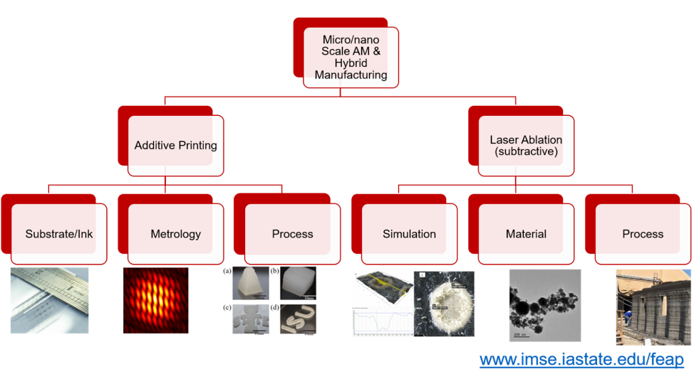
Citations